GeForce GTX 670 PCB Pictured In “Full” With Benchmark Results

With the Kepler GK104 cards, Nvidia’s aim has been low power draw and temperatures; the GeForce GTX 680 is the first top-end card we’ve seen for several years powered by only two 6-pin PCI-e power connectors. Being a slightly crippled version of its bigger brother, the GTX 670 improves upon this and has (for what it is) a truly tiny PCB, the reverse of which was seen recently when we looked at the Colorful GeForce GTX 670.
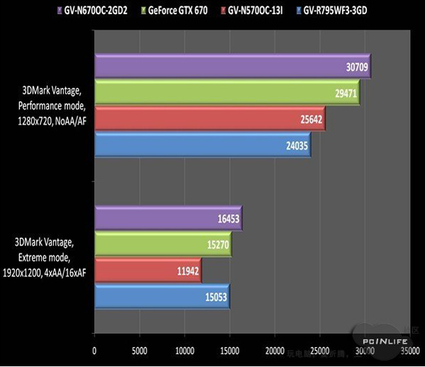
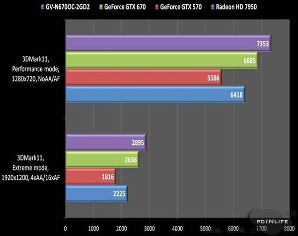
The GeForce GTX 670 has eight 2 Gbit memory chips spread equally over both sides of the PCB for a total of 2 GB of GDDR5 memory connected to the GPU by a 256-bit bus. In addition to this, the 4+2 phase VRM circuitry has been moved to the front of the card, sitting between the the GPU itself and the display connectors. These include two dual-link DVI ports, HDMI and DisplayPort. Along the top of the card you can see two SLI fingers, which allow for 4-way SLI capabilities and two 6-pin PCI-e power connectors which, unlike on the GTX 680, sit side-by-side. A PCinLife forum member by the name of “a269799355” posted benchmark results which follow below. Source — PCinLife Forums